
Title:
Plenary Speaker
Dr. Yuvaraja Visagathilagar
Principal Engineer at QinetiQ, Australia
Abstract
Biography
Dr Yuvaraja Visagathilagar has over 27+ years of extensive expertise and experience in academia, research, and industry. He graduated with Bachelor of Engineering in Communication Engineering and Doctorate in Engineering (with a highly prestigious scholarship from the Australian Government) in 1996 and 2003 respectively from RMIT University, Melbourne Australia. His dissertation was in “Narrow-band Optical Modulator on Lithium Niobate” for telecommunication applications but it can be applied for other transceivers applications. In research and industry, he has contributed to over 40+ peer-reviewed international journals and conference pubications. He has visited and presented at universities in USA (i.e. UCLA and UCSD), Peregrine Semiconductor Corporation and in Japan (i.e. Science and technology Organisation).He has collaborated with Defence Science Technology Organisation (now DSTG) in Australia where he has contributed in the design, fabrication, packaging and testing of “High-Speed Lithium Niobate Optical Modulator” including documentation of processes for quality certification (ISO 9001) and flip-chip packaging of narrow-band optical modulators on Lithium Niobate and Ceramic materials. He has extensive academic teaching as a lecturer and post-doctorate research fellow in Photonics, Fibre Optics & System, RF System, and Integration where he was involved in research of novel design of narrowband optical modulators. In early years, his research has been in Narrow-band Lithium Niobate Modulators but also in finding a solution for packaging of optoelectronic devices (i.e. ceramic and Silicon materials). During the collaboration, he worked with sub-contractors in system integration and packaging of the modulator devices in hermetically sealed packages for defence applications. In 2006, he joined “Future Fibre Technologies Ltd” who are the global leading organisation in optical sensing technologies and has extensive experience over 9 years in optical sensing. He was a senior manager and held positions as Senior Fibre Systems Engineer, R&D Team Leader and Applications Engineering Manager where he contributed in the company products enhancements and novel products design. He has contributed to 2 patent solutions for novel systems in optical fibre sensing and contributed to over 110+ reports with fellow colleagues and R&D teams (not published due to commercial-in-confidence). From July 2016 to March 2018, he was a Senior Academic at RMIT University for postgraduate and undergraduate courses in Electrical Engineering Analysis using Matlab, Electronic Engineering, Radar technologies, Communication systems, Optical/Photonic Engineering, Microwave Circuits & System and Advanced Mathematics for various program levels (or years). He contributed to the development teaching materials of a core course in Optical Fibre Systems and Networks for Bachelor and Master’s Program including supervising for over 10+ projects in undergraduate and postgraduate students with a minor thesis. Since April 2018 to June 2020, he is a Senior Academic with the Department of Electrical and Electronics Technology & Engineering, Applied Engineering College (AEC), Riyadh, Kingdom of Saudi Arabia which is affiliated with Lincoln College International and University of Hull, UK with accreditation of Colleges of Excellence by the Government of Kingdom of Saudi Arabia where he is undertaking teaching in Electrical and Electronics technologies & principles for various Bachelor level program. He has been a senior supervisor for over 30+ projects demonstrated and a minor thesis. In July 2020, he is a researcher undertaking photonics research into reservoir computing and senior academic in lecturing a topic in Optical Fibre Communication Systems, Digital Electronics projects using Altium to design & built a Digital Oscilloscope and Microwave/RF Systems with ©Cadence and Electronic Engineering at the University of Melbourne (Australia) and in January 2021, he joined RMIT University as a researcher and senior academic undertaking research in optical fibre systems and transmission with high-level multi-disciplinary engineering team. Since January 2022, he joined QinetiQ Australia as a Principal Engineer (Senior RF/EMI/EMC Systems Engineer) as a Design and Advisory role providing his expertise & experience in defence and government projects with key interest in Microwave/RF/Radar Communication Engineering, coherent detection optical sensing for pipelines, undersea exploration, seismic detection and temperature sensing, high-speed and narrow-band optical modulators. Recently in March 2023 was awarded with accreditation & certified with the Engineers Australia (EA) Chartered Professional Engineering (CPEng) and in the National Engineers Register (NER), APEC Engineer and IntPE(Aus). He has a distinguished professional engineering career, he is an active Senior Member of the IEEE for over 28+ years’ service where he is the Chair of the Victorian IEEE Electron Devices & Photonics Society Joint Chapter and representative in the Section Committee, Australia from 2017 He is a active member of IEEE where he is a key volunteer for the Senior Member Elevation reference in Victoria, Australia (or globally), Member of OSA, SPIE, AP-MTT, AIP, AOS, BCS and certified in PRINCE2® & system engineering. He is in various editorial boards for peer-reviewed international journals and key reviewer for many international scientific journals and conferences. He has presented at various international and local conferences as Plenary, Keynote, Invited and has been asked to provide a welcome talk at conference. Other interests include and on-going, provides professional engineering consultancy to organisations locally and globally but passionate about teaching high school students from year 7 – VCE & other states in all Mathematic, Physics, System Engineering and Technology.
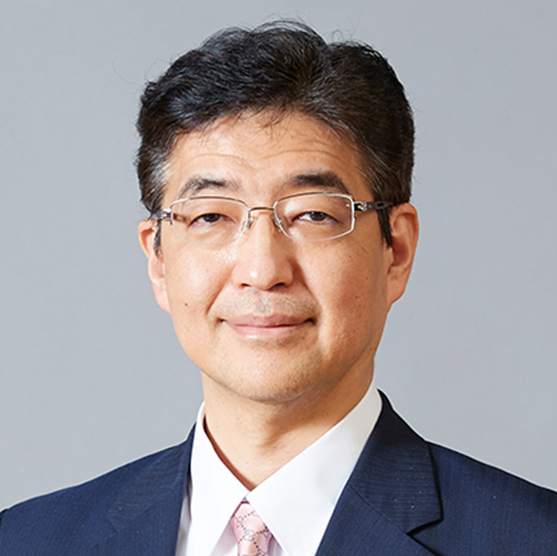
Title: Terahertz Photonics in 6G for Ultra-High-Speed Wireless Communication and Sensing Capabilities.
Speaker
Prof. Katsuhiro Ajito
International Professional University of Technology in Osaka Japan
Abstract
Terahertz Photonics in 6G: Ultra-High-Speed Wireless Communication, Sensing/Imaging Capabilities, and Smart Healthcare
Dean/Prof.Katsuhiro Ajito,
Department of Information Technology, Faculty of Technology, International Professional University of Technology in Osaka, JAPAN
Abstract:
With the sixth generation (6G), a wide frequency band is being considered for ultra-high-speed wireless communication. Within this band, extremely high frequencies known as sub-hertz or terahertz (THz = trillion hertz) radio waves ranging from 100 GHz to 3 THz are being explored. The use of higher radio frequencies is advantageous for high-speed data transfer because they exhibit light-like properties, such as higher directivity.
Base station antennas for higher radio frequency require the deployment of numerous antennas because of the narrower coverage area. The technology to be integrated into smartphones is still in the future, but commercial use in backhaul (relay lines connecting wireless base station antennas to the core communication network) and fronthaul (relay lines connecting wireless base stations and antenna units when they are separated) has already been standardized internationally in the 300 GHz band, specified as 252 GHz to 325 GHz, with a communication speed of 100 Gbps, by IEEE 802.15.3d-2017 in 2017.
Japan has been at the forefront of research in the 300 GHz band, with successful experimental demonstrations achieving 40 Gbps over 160 meters in the Japan-EU project called ThoR (TeraHertz end-to-end wireless systems supporting ultra-high data rate applications) from 2018 to 2022. Additionally, at the 2019 World Radio Conference (WRC), contributions from Japan, Germany, IEEE, and others led to the standardization of the 275 GHz to 450 GHz range under agenda item 1.15.
Furthermore, taking advantage of shorter wavelengths and higher light-like directivity, future developments are envisioned where wireless communication networks themselves possess sensing capabilities for applications such as positioning and object detection using radio frequencies. At 300 GHz, it is likely that ultra-precise positioning can be achieved even with errors on the wavelength scale. Additionally, smart healthcare using 6G network and 6G photonics are also discussed.
Biography
Katsuhiro Ajito received his Ph.D. degree in applied chemistry from the University of Tokyo, Japan, in 1995. He was a Distinguished Technical Member of THz-wave applications at NTT Science and Core Technology Laboratory Group in Atsugi, Japan. He joined NTT Basic Research Laboratories in 1995, where he conducted studies on glutamate in single synapses in the brain using Raman spectroscopy and laser tweezers from 1995 to 2007. His current research interests include terahertz photonics in 6G for ultra-high-speed wireless communication and sensing/imaging capabilities.In 1999, he was awarded the Young Scientist Award for the Presentation of an Excellent Paper from the Japan Society of Applied Physics (JSAP). From 1995 to 2019, he served as the Executive Director and Chair of the Terahertz Spectroscopy Division of the Spectroscopical Society of Japan (SSJ). He was also the Secretary of the Terahertz Interest Group in the IEEE 802.15 Working Group for wireless personal area networks from 2011 to 2013 and the Chair of the Micro/Nano Electromechanical Systems and Bio/Medical Analyses Area of the International Conference on Solid State Devices and Materials in JSAP from 2012 to 2015. Since 2021, he has been working at the Department of Information Technology, Faculty of Technology, International Professional University of Technology in Osaka, serving as the Chair, and has been the Dean since 2022. He is a member of IEEE, JSAP, SSJ, and the American Chemical Society.
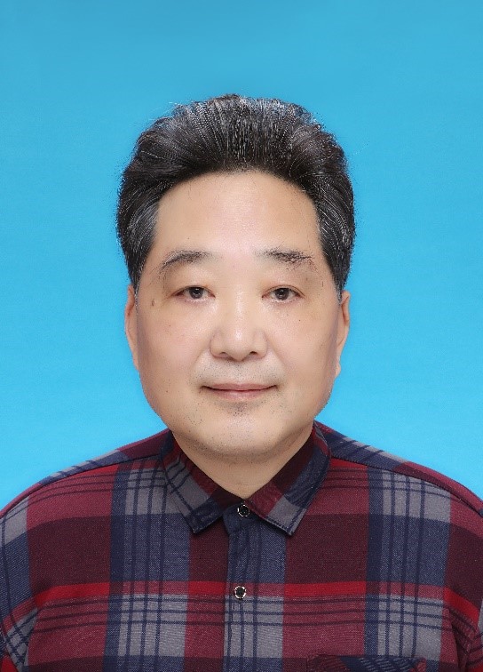
Title: Design and Implementation of an Integrated Airborne Laser Tracking and Communication System
Keynote Presentation
Prof. Dr. Xizheng Ke
Xi'an University of Technology, China
Abstract
The small and portable drone relay system is an important component of airborne laser communication and a prerequisite for maintaining normal communication links. This article proposes a non-confocal axis alignment method for airborne laser communication, and designs and implements an airborne laser tracking communication system. The system consists of a ground transmitting end and an airborne relay end. The ground transmitting end uses a camera and a pan head for image tracking. The airborne relay end uses a four quadrant detector as the detection unit, and a micro motor as the control servo system to control the two-dimensional mirror with a large dynamic adjustment range to adjust the beam and achieve non confocal axis alignment between the receiving and transmitting sides. The avalanche photodiode is used as the communication unit. On this basis, airborne laser communication experiments were conducted. The experimental results show that the tracking accuracy of the system is 13.98 μrad, and the amplitude of the electrical signal output by the signal detector is 23.0 mV. This method can achieve alignment without the need for data retrieval, and can quickly establish a transmission link while also achieving the establishment of a reverse link, without the need for an air stable platform. The feasibility of applying this method to airborne laser communication systems has been verified.
Biography
Xizheng Ke, Ph.D., Second-level Professor, deputy director of Shaanxi Provincial Key Laboratory of Intelligent Cooperative Network Military-civilian Joint Construction. Famous Teaching Teacher of Shaanxi Province, Fellow of Chinese Institute of Electronics, Foreign academician of Russian Academy of Natural Sciences, Director of Chinese Optical Engineering Society, Standing Director of Shaanxi Optical Society.
Title: Controlling the Brain and Heart with Light
Plenary Presentation
Prof. Sukhdev Roy
Head of the Department, Dayalbagh Educational Institute, India
Abstract
Optogenetics has made a strong impact in neuroscience by providing unprecedented spatiotemporal resolution in reading and writing neural codes with relatively lower invasiveness. In optogenetics, a genetically encoded light-sensitive protein is introduced into cells to make them sensitive to light. The expressed protein generates either inward or outward current in the presence of light, and can reversibly change the cell membrane voltage. Thus, the activity of these cells can be controlled and monitored with light. Optogenetics also enables all-optical control and recording of cellular activity in living tissue and opens up exciting prospects for optical neural prostheses. Recently, the first successful human trial of optogenetic retinal prostheses and promising results in cardiac optogenetics have been demonstrated.
Computational modelling of optogenetic systems has made significant contributions in developing a better understanding of the photocurrent dynamics in opsin molecules and the change in membrane potential in opsin-expressing cells in response to light. Computational models help in quick virtual testing of newly developed light-sensitive proteins in different cell types within realistic tissue and organ-level settings.
The talk would focus on our recent research in computational optogenetics for low-power, high-fidelity and high-frequency excitation, inhibition and bidirectional control of different neurons in the brain and cardiomyocytes in the heart, with newly discovered light-sensitive proteins and opsin pairs. The study not only provides a better understanding of the mechanism to efficiently control different cells but also allows optimization of their response.
Desensitization of photocurrent is a fundamental problem while using faster opsins. Under sustained illumination, the photocurrent in fast opsins desensitizes with time and results in spike failure below a certain threshold. Recently, we have shown that co-expressing step function opsins with fast channelrhodopsins can overcome this challenge. It has also been shown that ultra-low power deep sustained optogenetic excitation or suppression of electrical activity in human cardiomyocytes can be achieved with the newly discovered ChRmine opsin. The future prospects of optogenetics will also be discussed.
Biography
Professor Sukhdev Roy received the theBSc (Hons) Physics degree from Delhi Univ, in 1986, MSc Physics from DEL in 1988, and PhD from ift Delhi in1993. He joined the DayalbaghEducational Institute in 1993, where he is at present the Head of theDepartment of Physics and ComputerScience. He has been a Visiting Professor at many universities that include, including Harvard (USA) Waterloo(Canada), Würzburgand Regensburg (Germany) Osakajapan) City University, and Queen Mary University of London (UK) TIFF, Mumbai, and Sc Bangalore (india). He has also been an Associate of the international Centre for Theoretical Physics, Trieste, Italy, and is a Member of the Global Panel of MIT Technology Review, Prof. Roy has made significant contributions in Photonics that encompass nano-blo-photonics, silicon and neuro photonics, fiber optics, and optical computing. His experimental and theoretical research on nano-bio-photonic systems that includes low-power and high-frequency optogenetic control of neural spiking, defines a new paradigm of technological convergence and innovation and opens up fascinating prospects for energy-efficient, ultrafast and low cost all-optical information processing sensing energy conversion, and healthcare. He has won a number of awards and fellowships that include, the AICTE Career Award for Young Teachers in 2001, 15PS Invitation Fellowship, japan in 2004, HC Shah Research Endowment Prize by Sardar Patel University in 2006, 1st IETE BB Sen Memorial Award in 2007, IETE-Conference on Emerging Optoelectronic Technologies Award in 2012, IETE-M Rathore Memorial Award in 2016, the Systems Society of India's National Systems Gold Medal in 2016, and the Distinguished Alumni Award by the Dayalbagh Educational Institute in 2021. He also has been awarded seven best paper awards in international and national conferences. He has published 175 research papers in reputed journals and conference proceedings and 11 book chapters. He chaired the 8th World Conference and Expo on Nanoscience and Nanotechnology, Philadelphia, the USA in 2020. He has delivered more than 100 invited talks in India and abroad that include Keynote Addresses and Plenary Talks at International Conferences that include the prestigious international Year of Light.commemorative Keynote Address at the 38th Convocation of the International Council of Academies of Engineering and Technological Sciences (CAETSL in 2015 and at the Annual Meeting of American Physical Society in 2008. He was the Guest Editor of the March 2011 Special issue of ET Circuits. Devices and Systems Journal 10 on Optical Computing. He is an Associate Editor of IEEE Access and is a member of the Editorial Board of Optics and Photonics journal He is also a Senior Member of IEEE (USA) and a Fellow of the Indian National Academy of Engineering, the National Academy of Sciences India, IETE (India), and the Optical Society of India. He is listed in the recent Stanford researchers study of Top 2% in World Ranking of Scientists-2020, in Optoelectronics and Photonics.
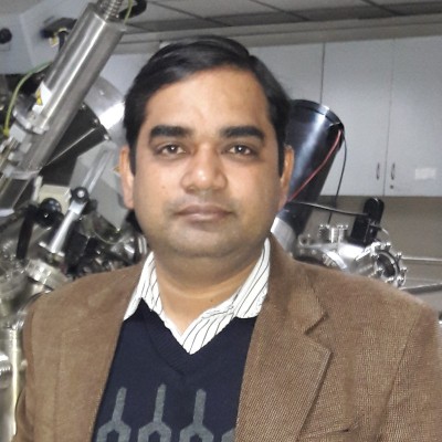
Title: Keynote Speaker
Synthesis of Semiconductor Heterostructures for Optoelectronic DevicesProf. Dr. Govind Gupta is a Senior Principal Scientist & Head Sensor Devices & Metrology Group at CSIR-National Physical Laborator
Prof. Govind Gupta
CSIR-National Physical Laboratory, India
Abstract
Synthesis of Semiconductor Heterostructures for Optoelectronic Devices
Prof. Dr. Govind Gupta1,2
1Sensor Devices & Metrology Group, CSIR - National Physical Laboratory (CSIR-NPL), Dr K. S. Krishnan Road, New Delhi 110012, India
2Academy of Scientific & Innovative Research, (AcSIR), CSIR-HRDC Campus, Ghaziabad, Uttar Pradesh 201002, India
Heterostructure-based devices have shown great potential in various fields, including electronics, photonics, and sensing. Semiconductor heterostructures were grown by physical & chemical vapor evaporation techniques. A variety of optoelectronic devices have been designed and fabricated with unique morphology exhibiting higher photocurrent generation and significantly enhanced responsiveness optical illumination. The developed device taps the broad wavelength range from Deep UV to the Mid-NIR spectrum. The fabricated device exhibits a substantially low dark current and fast time-correlated transient response and very high photo responsivity in a self-powered mode of operation. These devices demonstrate broadband optical response with state-of-the-art performance parameters in the photovoltaic and photoconductive modes of operation. I’ll discuss some of our recent findings in detail with possible mechanisms.
Biography
Prof. Dr. Govind Gupta is a Senior Principal Scientist & Head Sensor Devices & Metrology Group at CSIR-National Physical Laboratory, A National Measurement Institute of India, New Delhi, India & Professor Academy of Scientific & Innovative Research (AcSIR), India. His core area of expertise is the growth of exotic semiconducting materials, including nitrides, metal oxide & two-dimensional materials. Dr. Govind is developing intelligent and highly responsive optical sensors to detect harmful electromagnetic radiations and gas sensors to detect environmental pollutant gases. He has published more than 295 research articles in high-impact international scientific journals with more than 6200 citations and 9 book/book chapters. He is an elected Fellow of the Royal Society of Chemistry, UK (FRSC), Fellow of the Institute of Physics, UK (FInstP), Fellow of the Institute of Electronics & Telecommunication Engineers, India (FIETE), Fellow of Electron Microscopy Society of India (FEMSI), Senior Member of IEEE, USA (SMIEEE), and Associate Academician of the Asia Pacific Academy of Materials (APAM). Recently, he has been awarded International Exchange Award by one of the most prestigious, the Royal Society, UK, for performing collaborated research at the University of Cambridge, UK. Besides, he has been conferred numerous awards, including the Material Research Society of India (MRSI) medal, the Young Scientist Medal from National Academy of Sciences, India (NASI), BOYSCAST fellowship and Young Scientist Project Award from Ministry of Science & Technology, India, etc. He is also a visiting scientist to prestigious universities worldwide, including the University of Rutgers, New Jersey, USA, and Humboldt University, Berlin, Germany.

Title: 3D Co-Packaged Photonics Assembly Challenges and Solutions
Speaker
Dr. Jonas G. Croissant
IC Packaging Technical Program Manager USA
Abstract
Photonic optical co-packaging can increase the interconnecting bandwidth density and energy efficiency for quantum computing, 5G, and AI applications, and datacenter interconnections. One of the main challenges to making such advanced packages is to develop a high-yielding and scalable assembly process for cost-effective high-volume manufacturing. In this presentation, we will investigate a selected Intel co-packaged photonic assembly, and its various components and discuss several assembly challenges and their solutions. Specifically, dispense, chip attach, and Laurentide coupler attach strategies will be presented to manage 3D stacking warpage and product reliability.
Biography
Jonas G. Croissant completed his PhD in chemistry, materials science and engineering from the Ecole Nationale Superieure de Chimie in Montpellier (France) in 2014 and then conducted joint post-doctoral studies at King Abdullah University of Science and Technology (KAUST, Saudi Arabia) and the University of California, Los Angeles (UCLA, USA, CA). From 2017 to 2019, he was a professor of chemical engineering at the University of New Mexico (UNM, USA, NM). Since 2019, he joined Intel Corporation’s technology development organization and now focuses on the prototype-to-HVM innovation of photonic optical co-packaging assembly for next-generation products. He holds five Intel packaging patents, his silica hybrid nanomaterials and films research yielded 50 peer-reviewed publications, 3 book chapters, and 2 patents, and has served as an expert reviewer for European funding agencies and top global peer-reviewed publishing groups (e.g. Nature Publishing Group).

Title: Keynote Speaker
Uniting Distant Atoms: Exploring Shared Radiant Modes in Nanophotonic Waveguides
Hamidreza Siampour
Queen's University Belfast, UK
Abstract
Uniting Distant Atoms: Exploring Shared Radiant Modes in Nanophotonic Waveguides
Hamidreza Siampour
Centre for Quantum Materials and Technologies, School of Mathematics and Physics, Queen’s University Belfast, Belfast BT7 1NN, UK
In this abstract, we highlight recent advancements in the field of nanophotonic waveguides for quantum optical devices and their potential for quantum communication and sensing.
In the first part, I discuss the development of integrated quantum photonic circuits based on dielectric-loaded plasmonic waveguides with accurately positioned nanodiamonds containing single vacancy centers [1-4]. By combining resonant and plasmonic enhancement, we significantly increase the spontaneous emission rate of single photons.
Moving on to the second part, I present a chiral nanophotonic waveguide platform with embedded quantum dots that enables both Purcell-enhanced emission and strong chiral coupling. We observe record-high Purcell factors for quantum dots emitting in the slow-light spectral region, and demonstrate chiral routing of spin-carrying photons with exceptional Purcell factors [5].
These advancements, combining plasmonic and photonic crystal waveguide modes, enable strong bonding through radiation coupling in a shared mode. They pave the way for nanoscale functional quantum devices and scalable quantum optical networks.
Biography
H. Siampour is currently a Lecturer at Queen's University Belfast, where his research primarily revolves around investigating the interplay between nanophotonics and quantum optics. Before his current role, he held the position of Research Associate at the University of Cambridge, working on the development of a quantum simulation platform using interacting spins in diamond. Prior to that, he was a Postdoc at the University of Sheffield, working on the development of a semiconductor nanophotonic platform for directional spin-photon coupling. He obtained his PhD degree in Nano-optics from the University of Southern Denmark, with his thesis titled "A Nanophotonic Platform for Quantum Optical Integrated Circuits"
Title: A Comparative Study of the Chemical Bonds of ZnO Rocksalt and Wurtzite types Under Extended Pressure and Temperature; a Molecular Dynamics prediction
Speaker Presentation
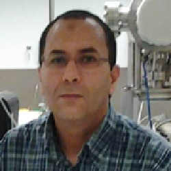
Dr. Yahia Chergui
Assistant Professor, University M’Hamad Bougara of Boumerdes, Algeria
Abstract
Zinc Oxide is still an important substance in macroscale and nanoscale due to the huge properties under different pressures and temperatures, because of its chemical bonds are between covalent and ionic. In this work we are analyzed the behaviour of zinc oxide rocksalt and wurtzite behavior under the range of pressure 0-100GPa and the range of temperature 300-3000K. We are investigated Molecular Dynamics and DL_POLY on Raven Supercomputer of Cardiff Universityin UK to compare between these bonds under previous conditions. We are used 9a x 9b x 9c as a dimension of our simulation box; we used 5832 atoms of rocksalt and 2916 atoms of wurtzite. Our results are in the vicinity of available data; this information is very important in many industrial fields.
Biography
Yahia CHERGUI is an assistant Professor in Electrical & Electronics Engineering Institute, Boumerdes Algeria. He has completed his PhD from Badji Mokhtar University in Annaba, Algeria. He did all his PhD work in Cardiff University in UK. His research field is Physics(condensed matter, and soft matter simulation by molecular dynamics). He has many published articles and international conferences. He has been serving as a referee with condensed matter journal (IOP), Energy journal (Elsevier), and American Journal of Modern Physics.

Title: Plasmonic Gold Nanoparticles and Rose Bengal Dye Synergy in Fiber-Optic Humidity Sensor Design
Keynote Presentation
Prof. Sib Krishna Ghoshal
University of Technology Malaysia, Malaysia
Abstract
Demand of high perfromance and inexpensive fiber-optic relative humidity sensors (FO-RHS) with rapid response are ever-increasing. Compared to the conventional sensors, the FO-RHS are beneficial because of their simple operation, high stability and efficient signal detection. Despite the existence of various chemiresistive humidity and gas sensors made of polymers and hybrid inorganic/organic nanomaterials, a high quality RHS with excellent linearity, short response time, and low hysteresis remains deficient. The health-care and food processing sectors worldwide need ultrasensitive materials for RHS making, proposing various compact designs like side-polished, tapered, and hetero-core fibers. Presently, the functionalized gold nanoparticles (AuNPs)-incorporated fluorescent organic molecules are used as real-time humidity biosensors for respiratory diseases diagnoses. Commercially accessible RHS materials including electrolytes, organic polymers, and ceramics have issues involving sensitivity, reversibility or medical resistance. Rose Bengal dyes (RBD) are excellent photosensitizers owing to their several notable attributes. Thus, the pruned triangular AuNPs (with enhanced fluorescence and LSPR absorption) surface were modified by RBD molecules for more water molecules adsorption and extra charge carriers trapping at the metal-semiconductor Schottky contact thereby improving the RHS response. The synergy between nanosized receptor layers and optical fiber platform was established to provide a strong humidly sensing trait. These stable RBD molecules-decorated AuNPs grown at optimum laser fluence by PLAL method showed better sensitivity and linearity than the one coated with pure AuNPs when tested against polyvinyl alcohol. Strong attachment of –OH and COOH functional groups of RBD onto AuNPs surface was responsible for PVA molecules sensing via the hydrogen bonds formation.
Biography
Dr. Sib Krishna Ghoshal is currently Associate Professor of Physics at the Faculty of Science, University Technology Malaysia since 2010. From 2004-2010 worked in the Physics Department and Materials Science Program of Addis Ababa University, Ethiopia, Africa as Associate Professor in the United Nations Development Program for the expansion of Graduate Studies. He served as senior lecturer and promoted as reader at Guru Jambheshwar University of Science and Technology, India during 1998-2006. He received PhD degree in Condensed Matter & Statistical Physics in 1996 from School Physical Sciences, Jawaharlal Nehru University (Delhi, India). Carried out two post-doctoral researches one in Martin Fisher School of Physics (Brandeis University, USA) during 1999-2000 and the other in a joint research project of Indian Institute of Technology (Delhi) & Oxford University (UK) in 1996-1998. Supervised few Master Theses with Nicola Marzari (MIT, USA) and worked with Sir Roger Elliotte (Oxford, UK). He received Master Degree in Physics in 1989 from Premier Presidency University, Calcutta and BSc (Physics Honors) degree in 1986 from Calcutta University. Besides having a long innings-spanning almost three decades in teaching Physics/Materials Sciences at various levels and advising an appreciable number of doctoral and masters theses, he possesses a remarkable research profile too. He published over 600 research articles (334 in Journals with total impact factor of 660), 15 book chapters, and 7 books. His Google scholar h-index is 38, i10-index is 111 and citations are 4691. So far, he received 55 research grants, supervised 25 PhD, 80 MSc, and 65 undergraduate theses. He is listed as top 2% scientists in physics worldwide in 2020. His recent research interests are in Advanced Optical Materials, Statistical Condensed Matter Physics, Nanomaterials Syntheses and Applications, Laser Physics, Simulation and Modeling as well as Nanoscience. One of his major concerns other than research pursuits is the social impact of science and technology on environment, marginalized societal groups deprived of higher education, and the imbalances thereupon in the distribution of its fruits and adverse impacts on these stakeholders.
Title: Excitons in semiconductor single crystals and quantum dots
Plenary Presentation
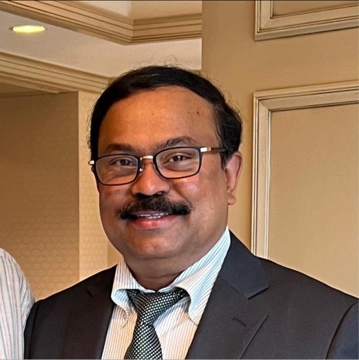
Prof. Vasudevanpillai Biju
Hokkaido University, Japan
Abstract
will be updated soon…
Biography
Vasudevanpillai Biju is a Professor and the Director of the Promotion Office of International Alliance at the Research Institute for Electronic Science and Graduate School of Environmental Science at Hokkaido University. He assumed this position after a research career as a scientist and a senior scientist at AIST, Japan (2004-2015), a PRESTO researcher at Japan Science and Technology Agency (JST, 2010-2014), a visiting Scientist at the University of Texas at Austin, USA (2007), a postdoctoral fellow at Pacific Northwest National Laboratory, USA (2003-2004), a JSPS postdoctoral fellow at AIST, Japan (2002-2003), and a research scientist at Angstrom Technology Partnership, Japan (2000-2002). He has been a visiting faculty at many universities in Japan, the US, and India. He has been a member of the board of studies/faculty evaluation/faculty screening/project screening committees of academic and government bodies in Japan, India, New Zealand, Chili, Taiwan, the European Union, Singapore, Belgium, etc. He has been a SPARC fellow at IIT Hyderabad, India, and an Erudite Fellow of the Bard of Higher Education, Kerala, India. His research interests include semiconductor nanocrystals and quantum dots, photo-functional molecules, nanobiotechnogy, and single-molecule techniques. His research activities are recognized with various awards by the Ozaki Foundation (Gen-nai Prize and Gen-nai Award), the Japanese Photochemistry Association, the Asian and Oceanian Photochemistry Association, and the Chemical Society of Japan. He became a Fellow of the Royal Society of Chemistry in 2011. He has been an associate editor of J. Photochem. Photobiol. C, and NPG Asia Materials.
Title: Methylthio-substituted coumarin-based fluorescent probe for highly specific and fast detection of hypochlorite
Keynote Presentation
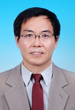
Prof. Hongqi Li
Donghua University, China
Abstract
Hypochlorite ion plays a critical role in physiological processes and is very important for killing bacteria that invade the immune system of organisms. The abnormal level of hypochlorite ion in the living organism can result in a host of health problems including cardiovascular diseases, acute lung injury, Alzheimer’s disease, respiratory distress, inflammation, and even cancer. Therefore development of efficient methods for sensing of hypochlorite is of high significance. Detection of hypochlorite by using fluorescent probes is a prominent technique because of their good sensitivity, specificity, fast response and temporal and spatial resolution for real-time imaging. In this work a methylthio-substituted coumarin-based probe was designed and synthesized for fluorescence turn-off detection of hypochlorite in MeCN/PBS solution (4:6, v/v, 10 mM, pH 7.4). The probe displayed an excellent selectivity over other competing species and featured a fast response time of less than 20 seconds. The detection limit was estimated to be 0.47 μM while the applicable range for sensing hypochlorite by the probe was pH 4-10. Thus this approach provided a new type of fluorescence turn-off probe for rapid, highly sensitive and selective detection of hypochlorite in an aqueous solution.
Biography
Hongqi Li obtained his PhD degree from Lanzhou Institute of Chemical Physics, Chinese Academy of Sciences. He was a guest researcher in Kyoto University (1999‒2001), Ehime University (2002‒2003) and CNRS-University of Aix-Marseille I & III (2003‒2004). He has been working as an Associate Professor in College of Chemistry and Chemical Engineering, Donghua University since 2004. His research interest is focused on organic functional dyes and fluorescent sensors. He has published more than 130 papers in accademic journals.
Title: Plenary Talk
Recent Trends in Optical Fiber Sensor Technology
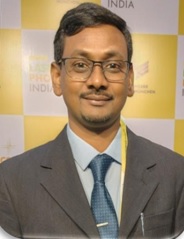
Dr. Philip B. Kassey
Founder & Managing Director of PETRASYS GLOBAL PVT LTD ,India
Abstract
Recent Trends in Optical Fiber Sensor Technology Philip B. Kassey1 Petrasys Global Pvt Ltd.,#89, Love Villa, Sector-2B, Airoli, Navi Mumbai -400709, India *philip@petrasys.com ABSTRACT Optical fiber sensors (OFS) are a type of technology that enables the sensing and measurement of various physical parameters, including temperature, strain, pressure, and more. While OFS technology has been in existence for several years, recent advancements have significantly enhanced its performance and opened up new applications. One of the latest trends in OFS technology is the emergence of distributed sensors. Unlike traditional sensors that can only measure specific locations, distributed sensors can continuously monitor entire structures such as pipelines or bridges. This represents a significant improvement in monitoring capabilities. Additionally, OFS technology has made strides in achieving high-precision sensing with exceptional resolutions, reaching sub-micro strain and sub-micron levels. This heightened sensitivity enables the detection of even subtle changes in physical parameters. Integration of OFS with other technologies, notably micro-electromechanical systems (MEMS), is another prominent trend. This integration enables sensing in harsh environments and enhances overall sensing capabilities. For instance, OFS can be integrated with MEMS to create miniature sensors that can be implanted inside the body to monitor vital parameters in critical care patients. OFS are finding applications in a diverse range of fields, including healthcare, aerospace, and civil engineering. In healthcare, OFS are utilized in biomedical imaging and the monitoring of vital signs. In the aerospace industry, OFS play a crucial role in the structural health monitoring of aircraft. In civil engineering, OFS are employed for the monitoring of bridges, tunnels, and dams, enabling effective structural health monitoring. In conclusion, the recent advancements in OFS technology have resulted in improved sensing capabilities, heightened sensitivity, and real-time monitoring of structures. Continued research in this field is expected to further propel the development of novel sensing applications with OFS playing a vital role. Keywords: Optical Fiber; Sensor; Distributed; Acoustic
Biography
Dr. Philip B. Kassey, Founder & Managing Director of PETRASYS GLOBAL PVT LTD, Mumbai, India. With over 20 years’ Industrial and Academic Experience in the field of Fiber Optic Sensor Systems Research, Design, Development & Production in India & Abroad. Career started as a researcher, and worked at different levels as a Scientist, Engineer, Academician, Technology Architect, and Entrepreneur, which led to excel as a Business Owner, Trainer and Coach in Photonic Sensor Technology. Conducted several technical trainings sessions in India, Seychelles, London, and USA. Industrial Expert in Optoelectronics, Photonics and Fiber Optics Sensors. Mind behind the Development of Fiber Optic Perimeter Intrusion Detection System for Border Security, India. Industrial Expert in Optoelectronics, Photonics and Fiber Optics Sensors. In the area of Perimeter, Border Security & Surveillance, protection of Forest Animal and Human conflicts as well as conservation of Tigers and monitoring the movement of the extinguishing animals in the forest reserves.

Title: Charactarizing Electronic Component for Space Radaiation Environment
Speaker
Dr. Manzar Mahmud
Avionics and Space Radiation Researcher Canada
Abstract
Charactarizing Electronic Component for Space Radaiation Environment
Manzar Mahmud
MDA Space, Brampton, Ontario, Canada
The type and magnitude of radiation effects observed in electronics are largely defined by specific device properties and the radiation environment in which the devices are used. It is important to know radiation environment to characterize the electronic component. Depending on radiation environment and orbit type, avionics may experience differenet kinds of radiation effect. To characterize radiation hard electronics, different kids of radiation testing needs to be performed. This talk will focus on the radaition environment, avilable testing facilities, and characteriztion of radiation hard electronucs.
Biography
Dr. Mahmud completed his Ph.D. in 2022 from electrical & computer engineering, LU. His PhD topic was “A Smart Sensor-based Online Condition Monitoring System for Induction Machine Fault Diagnosis”. PreAfter his Ph.D., he joined the Space and Robotics team of MDA Space. He is involved in building Canada’s flagship project on the International Space Station in deep space, “Canadram-3” and currently working with NASA’s deep space exploration plan named GATEWAY. His work focused on the radiation environment and characterization of electrical components.

Title: A vision inside the quantum of light
Keynote Presentation
Dr. JAYNSTEIN
CEO & Founder, and Principal Research Scientist in JAYNSTEIN LLC, USA
Abstract
This rule could be described as: A vision inside the quantum of light
Æ ◎ яevolution is my third publication in which I will explain how the Multiverse generates the original force to create everything and transform energy to do it possibly. In this first rule that I call JAYNSTEIN Æ 123 Rule, I would like to show you how The Fifth Force, a new force never discovered by the current science was born. This new force is responsible for the transformation of energy. If I look back at when I started investigating the Æ or æther back in 2017 at Lake Tahoe with the spin of an orange, I realize the great breakthrough. First, knowing that The Fifth Force is the new force that comes from the union of two opposite polarities, and that gives rise to electromagnetism itself. My simplification is of such magnitude that with only two rules I can explain this. The first, JAYNSTEIN Æ 123 Rule describes how from a vacuum something can acquire a three-dimensional dimension, and the second, JAYNSTEIN Æ 369 Rule as its surroundings cause the generation of Electromagnetism.
Biography
I am the Founder & CEO of two Startups in Palo Alto, CA, and Mesa, AZ. Let me introduce what I did in these couple of business adventures. What is JAYNSTEIN Æ Model? My research during the last 5 years concluded in the summer of 2021 with the Best Young Scientist Award in Osaka, Japan, and some publications that I call JAYNSTEIN Æ Model. What is JAYNSTEIN Æ Tech? Now this research is transformed into new mindfulness devices that I call JAYNSTEIN Æ Tech. There are no competitors for these new mindfulness devices in the revolution of sports.
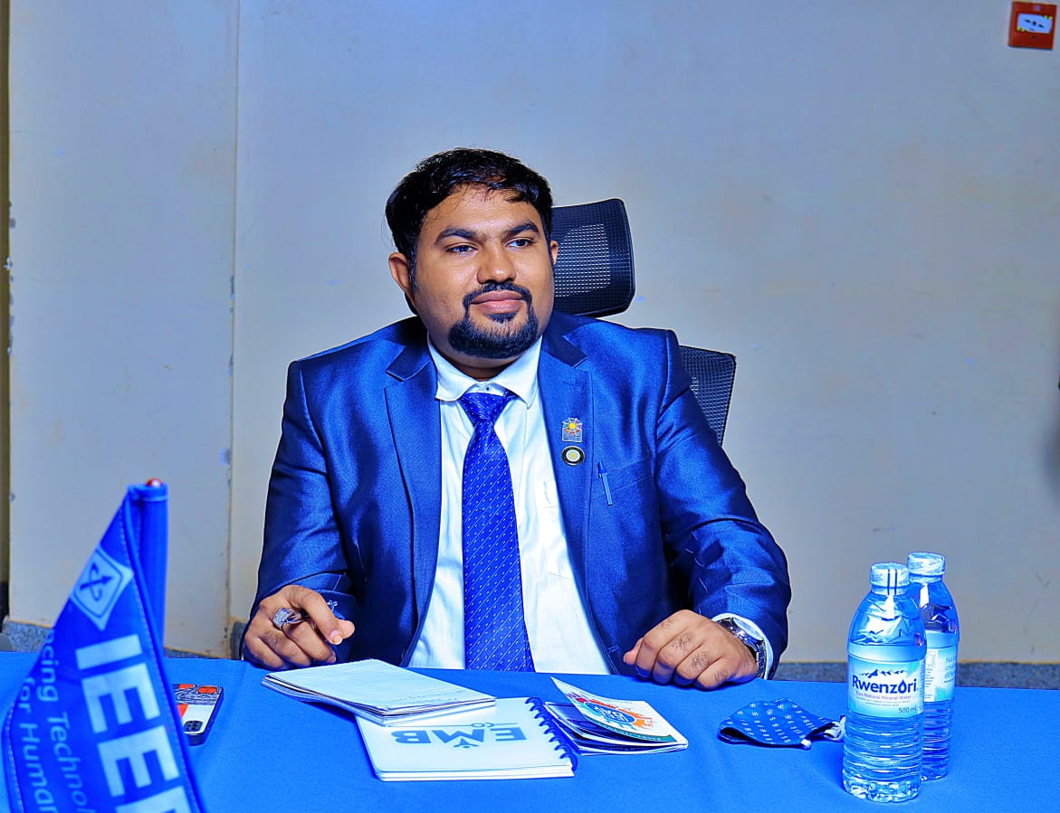
Title: Speaker
Photonic Crystal based Passive Devices for Photonic Integrated Circuits
Mayur Kumar Chhipa
ISBAT University, Africa
Abstract
Photonic Crystal based Passive Devices for Photonic Integrated Circuits
Mayur Kumar Chhipa, PhD, MIEEE
1Department of Electronics and Communication Engineering, ISBAT University, Kampala, Uganda
Integration of high-speed light devices, as well as technological advances, are critical factors influencing the development of integrated photonic circuits for optical communication networks. Every day, the increasing demand for wider bandwidth needs signal processing systems at high-speed. In conventional electronics, the signal processing speed is limited due to slow speed and huge power consumption. All-optical signal processing is an alternate way to increase signal processing speed at very low power consumption. Using the new generation of optical devices to perform all-optical logic operations with rapid transfer, storage, high processing speed, and high data rate, there are advantages to the realization of photonic integrated technology in comparison to the issues discussed in conventional electronic devices. Massive research is being conducted to design miniaturised photonic components for integrated circuits.
In general, photonic integrated circuits (PICs), are the combination of various photonics technologies like Photonic Crystals (PCs), Plasmonic, Planar Lightwave Circuits (PLCs) and Micro-Optical-Mechanical Systems (MOEMS). In comparison to the above discussed different platforms for PICs, photonic crystals-based devices are preferred because of their various advantages like ultra-compact in size, more temperature resilient, flexible design structure, low radiation losses, high operation speed, and very low group velocity.
Various photonic crystals based optical devices like: Channel Drop Filter, De-Multiplexer, Optical Switch, Optical Logic-Gates, Optical Encoder etc, will be discussed during the workshop and it has been observed that, further analysis could be done for different operating wavelengths and other parameters such as modifying the radius of rods, scatter rod radius or lattice constant. Such a device structure with low power consumption, small size and high data rate, which occupy less space could be utilized in future as photonic integrated circuits for high-speed optical communication.
Biography
Mayur Kumar Chhipa, serving as Lecturer and Coordinator at the department of Electronics and Communication Engineering, Faculty of ICT, ISBAT University, Kampala, Uganda, East Africa. He received his B. Tech and M. Tech degrees from Rajasthan Technical University in 2011 and 2015, respectively. He is author or coauthor of more than 25 research papers in reputed journals and conference proceedings. He has attended about 20 workshops and organized 10 workshops. He is a professional member of IEEE, IEEE Photonic Society, IEEE CAS, IEEE IES, OSI and IAENG. His current research interests are in the areas of Photonic Band Gap Structures, Optical Communication, Photonic Crystals, Photonic Integrated Circuits, Optical Devices, and Optical Communication Networks.
“ Will be updated soon...”
+91 9491 456 452
Door No.200, Immidhihalli Main Road, Whitefield-560066, Bangalore, India
About Us
Global Scientific Guild organizes conferences and webinars to promote quality research and real world impact in an atmosphere of true international co-operation between scientists, doctors, professors, practitioners, engineers and industry by bringing together the world class renowned personalities to discuss the latest developments and innovations at one common platform.